Introduction
Industrial, automotive, IT, and networking companies are major purchasers and consumers of power electronics, semiconductors, devices, and systems. These companies use the full array of available topologies for dc-to-dc converters that employ buck, boost, and SEPIC in different variations. In an ideal world, these companies or firms would use a specialized controller for each new project. However, adopting new chips requires significant investment due to the lengthy and costly process of testing new devices for compliance with automotive standards, verification functionality in the specific applications, conditions, and equipment. The obvious solution for reducing development and design cost is employing already approved and verified controllers in different applications.
The most used topology for generating a power supply is for step-down converters. However, employment of this topology is limited to generating positive outputs from the input voltages that are greater than the output. It cannot be used in a straightforward way for generating negative voltages or providing stable outputs when the input voltage drops below the output. Both aspects to generating output are important in automotive electronics when negative voltage is needed for supplying amplifiers or when a complete system must continuously work properly in case of cold cranking when the input voltage rails drop significantly. This article details a method for using a simple buck controller in SEPIC, Cuk, and boost converters.
Generating Negative and Positive Voltage from a Common Input Rail
Figure 1 illustrates the design of a bipolar power supply based on a single buck controller with two outputs.
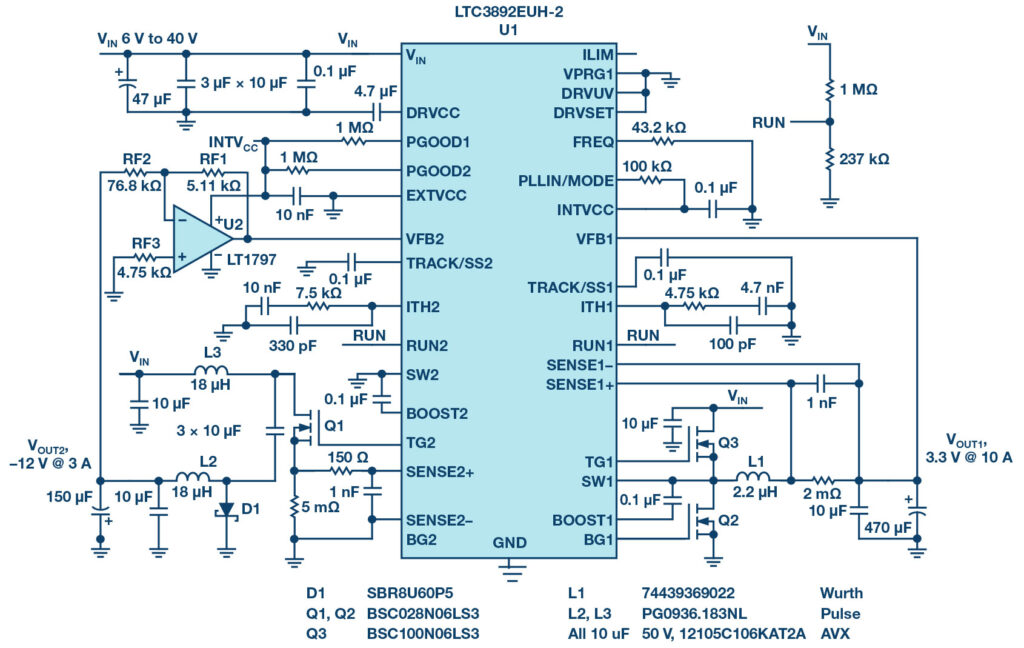
Figure 1. An electrical schematic of LTC3892 that is generating positive and negative voltages. VOUT1 is 3.3 V at 10 A and VOUT2 is –12 V at 3 A.
For maximum utilization of this chip, one output must be employed to generate a positive voltage and a second to generate negative voltage. The input voltage range of this circuit is 6 V to 40 V. The VOUT1 generates positive 3.3 V at 10 A and VOUT2 negative voltage –12 V at 3 A. Both outputs are controlled by U1. The first output VOUT1 is the straightforward buck converter. The second output has a more complex structure. Because VOUT2 is negative relative to GND, the differential amplifier U2 is employed to sense negative voltage and scale it to the 0.8 V reference. In this approach, both U1 and U2 are referenced to the system GND, which significantly simplifies the power supply’s control and functionality. The following expressions help to calculate the resistor values for RF2 and RF3 in case a different output voltage is required.
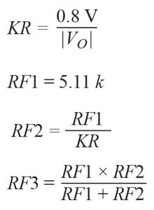
The VOUT2 power train employs a Cuk topology, which is widely covered in the relevant technical literature. The following basic equations are required to understand the voltage stress on the power train components.
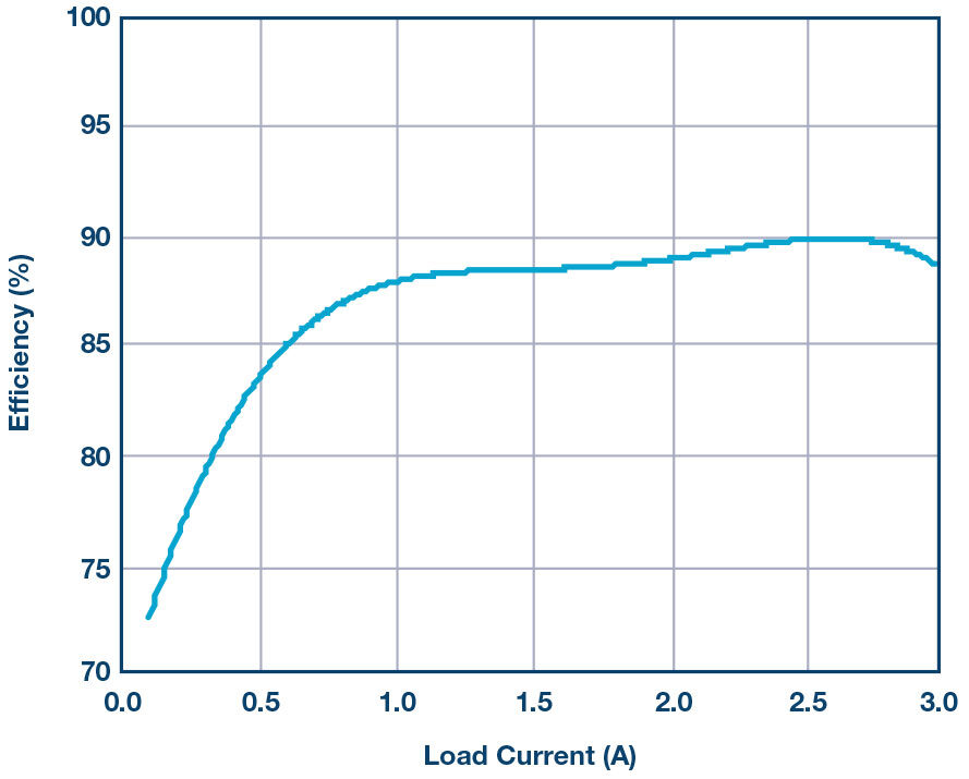
The VOUT2 efficiency curve is presented in Figure 2. The LTspice® simulation model of this approach is available here. In this example, the LTC3892 converter’s input is 10 V to 20 V. The output voltages are +5 V at 10 A and –5 V at 5 A.
Figure 2. Efficiency curve of the negative output at 14 V input voltage.
Generating Stable Voltages from a Fluctuating Input Rail
The electrical schematic of the converter shown in Figure 3 supports two outputs: VOUT1 with 3.3 V at 10 A and VOUT2 with 12 V at 3 A. The input voltage range is 6 V to 40 V. VOUT1 is created in a similar fashion, as shown in Figure 1. The second output is a SEPIC converter. This SEPIC converter, as with Cuk above, is based on noncoupled, dual discrete inductor solutions. Use of the discrete chocks significantly expands the range of the available magnetics, which is very important for cost-sensitive devices.
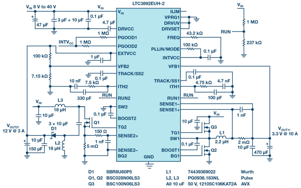
Figure 3. Electrical schematic of LTC3892 in a SEPIC and in buck applications.
Figure 4 and Figure 5 illustrate the functionality of this converter at voltage drops and spikes; for example, at cold cranking or load dumps. The rail voltage VIN drops or rises at a relatively nominal 12 V. However, both VOUT1 and VOUT2 stay in regulation and provide a stable power supply to the critical loads. The two-inductor SEPIC converter can be easily rewired to a single inductor boost converter
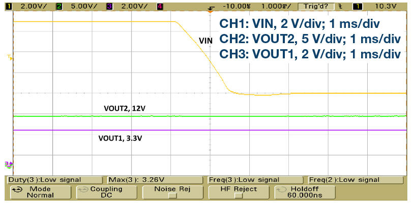
Figure 4. If the rail voltage drops from 14 V to 7 V, both VOUT1 and VOUT2 stay in regulation.
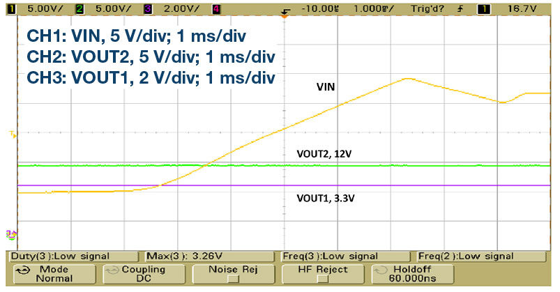
Figure 5. The rail voltage rises from 14 V to 24 V. However, both VOUT1 and VOUT2 stay in regulation
The relevant LTspice simulation model can be found here. It shows the LTC3892 converter’s input is 10 V to 20 V. The output voltages are +5 V at 10 A and –5 V at 5 A.
Conclusion
This article explained the methods of building bipolar and dual-output power supplies based on the step-down controller. This approach allows for the use of the same controller in buck, boost, SEPIC, and Cuk topologies. This is very important for vendors of automotive and industrial electronics, as they can design power supplies with a variety of output voltages based on the same controller, once it is approved.
Victor Khasiev [victor.khasiev@analog.com] is a senior applications engineer at ADI. Victor has extensive experience in power electronics both in ac-to-dc and dc-to-dc conversion. He holds two patents and has written multiple articles. These articles relate to the use of ADI semiconductors in automotive and industrial applications. They cover step-up, step-down, SEPIC, positive-to-negative, negative-to-negative, flyback, forward converters, and bidirectional backup supplies. His patents are about efficient power factor correction solutions and advanced gate drivers. Victor enjoys supporting ADI customers, answering questions about ADI products, designing and verifying power supply schematics, laying out print circuit boards, troubleshooting, and participating in testing final systems.